Monday, 21 October 2019

Test coverage, Fault coverage

Test coverage and Fault coverage are the two important quantities which measures how good the DFT logic was implemented on core design for controllability and observability of a design.

Test Coverage:
Test coverage is a measure of test quality of DFT, is the percentage of faults detected from among all testable faults. This is the number of most concern when you consider the testability of the design


Fault Coverage:
Fault Coverage consists of the percentage of faults detected from among all the faults that the test patterns generated by the tool


Where DT is detected faults class includes all the faults that the ATPG identifies as detected and this are classified into two groups

  • Det_simulation (DS)
  • Det_implication (DI)

PD – posdet or possible detected fault class includes all the faults that fault simulation identifies as possible detected but not hard to detect
Let us see how the test coverage and fault coverage was calculated from snap shot of status report

                                                  report_statistics of faults

From the report Total no of faults are given as 302778
Faults due to unused pins (UU), Tied pins (TI), Blocked Pins (BL), and redundant logic (RE) are untestable by tool and this faults must be excluded from the total number of faults while calculating the Test Coverage and considered while calculating the Fault Coverage.

UU+TI+BL+RE => 4984+1076+12+1072 = 7144

Thus Testable faults are given asTotal Faults – (UU+TI+BL+RE)
Total faults detected during simulation (DS) and implication (DI) are

DS +DI => 202752+75601+16 = 278369

In general posdet_credit will be set to zero and with this above faults numbers we can have Test Coverage and Fault Coverage


In this process TC and FC are calculated and we need to achieve 99 % Test Coverage for Stuck At fault model and 95% Test Coverage for At Speed fault model

Tuesday, 15 October 2019

Universal Gates

In one of my interview, the interviewer asked why AND, OR gates are not called as universal gates. I couldn’t answer to his question. Let us know why NAND and NOR gates alone called has Universal gates.

Universal Gates
A logic gate which can implement any Boolean function without need of other logic gates is called Universal Gate. From the above explanation we can conclude NAND and NOR gates as universal gates, which means we can implement any logic gates using these two gates.

Implementation of logic gates using NAND gate
1.       Inverter


2.       AND GATE 


3.       OR GATE


Implementation of logic gated using NOR gate

1.       Inverter 


2.       AND GATE


3.       OR GATE


AND, OR ,NOT which are basic gates can be implemented by using NAND or NOR gates as shown above, similarly any logic can be implemented using NAND or NOR gates. And so these gates are called universal gates.

When you are asked to  design a gate using one of the universal gate, which gate is better to use? 
NAND gate is more commonly used compared to NOR gate because they offer less delay compared to NOR gate and also occupy less area.

Friday, 11 October 2019

Multi Voltage Domain

Why we need the multi voltage domains in SOC, Can’t we design a chip with single voltage?
Yes we can design a chip with a single voltage when we are working on less frequency where speed is not main priority.

                                          Source : Internet

If someone is least interested in speed of operation like snail which will ultimately reach the destination but the time taken to reach the destination can be 1 hour or 5 hours, then we can design a SOC with single low voltage domain which operates at low frequency. And power consumption will be less as power is directly proportional to V2

If a person want the results in nano seconds, then the device must work at high frequency. With applying high voltage, high frequency can be achieved with a drawback of power loss, as power is directly proportional to V2

 Ex: Assume computer need to add 2 and 2, output will be 4. The time taken to execute the instruction and display the output depends on frequency of CPU, it will take more time if CPU is working on less frequency (low voltage). If the computer need to execute given instruction in nano seconds, the CPU should operate on high frequency (high voltage) with huge amount of power loss

Because of this huge power loss, it is not practical to design a SOC with single voltage domain at high frequency. To reduce the power consumption design was divided into multiple voltage or power domains each with its own supply voltage and this type of approach is called multi voltage design. The multi voltage design is based on realisation that in SOC design, different blocks will have different objectives for instance processor need to run at high speed and the processor block should be supplied with high supply voltage. On other hand USB block may run at fixed, relatively low frequency. In this case low supply voltage required for operation. Few blocks will be powered off when they are not in use.
Also multi voltages are required in RAM

  • Low voltage to maintain memory contents when the memory is not being accessed
  • Higher Voltage that supports read and write action

There are different Multi voltage domain strategies:

  • Static Voltage Scaling (SVS)
  • Multi-Level Voltage Scaling (MVS)
  • Dynamic Voltage and Frequency Scaling (DVFS)
  • Adaptive Voltage Scaling

To conclude, to reduce the power consumption at higher frequency, multi voltage domain is one of the technique used.

Thursday, 10 October 2019

N-type and P-type semiconductor

In semiconductor physics Group IV( in IUPAC Notation it is Group 14) contains Carbon (C), Silicon (Si), Germanium (Ge), Tin (sn), Lead (pb), Flerovium (Fl), all this elements contains 4 electrons in its outer shell nothing but four valence electrons. Out of all this elements Silicon (Si) is widely used in fabrications of chips because of following advantages.

  • Silicon reacts with oxygen and forms oxides itin a controlled manner and forming a layer of stable oxide which reduces thesurface recombination velocity
  • Its hardness that allows large wafer to behandled safely
  • Its thermal stability, up to 1100o C,that allows high temperature processing related to diffusion, oxidation andannealing
  • Primarily available for low cost

By adding an impurity conductivity of material can be increased and depending on the impurity added we can have two types of semi-conductors
N-type Semiconductor :
When the group V element is added to the intrinsic or pure semiconductor (silicon or Germanium), the resulted product is said to be an n-type semiconductors. The group V elements are phosphorus, arsenic, antimony and this elements have five valence electrons. When Phosphorus is added to silicon, it forms four covalent bonds with neighbouring silicon atoms. The fifth valence electron of phosphorus atom does not involve in formation of covalent bond and this electron is free to move in structure. As the group V elements donates a free electron, these elements are called donors. With small addition of impurity (phosphorous) provides millions of electrons which are majority carrier in n-type semiconductor

                                             N-Type Semiconductor

P-type Semiconductor
When the trivalent impurity or acceptor impurity added to Silicon (Group IV), the resulted product is said to be p-type semiconductors. The group III elements are Boron (B), Gallium (G), Indium (In), Aluminium (Al) and these elements has three valence electrons. When Boron in added to Silicon as impurity, three covalent bonds are formed with three neighbouring silicon atoms and in fourth covalent bond, only silicon atom contributes one valence electron, while the boron atom  is in short of one valence electron. Thus the fourth covalent bond is incomplete with shortage of electron and this missing electron is called hole. With small addition of impurity (boron) provides millions of holes which are majority carriers in p-type semiconductor

                                                       P-Type Semiconductor

Wednesday, 9 October 2019

VIM editor series II

Here is second post on the vi editor commands.
Insert a file content

:r file_name or file_path

example: Need to paste the info from file B to A      

           Copied the content to file A from file B using command :r B 

Repeat the Last Action 

. (dot or aka period or full stop)

  • Suppose you press dd to delete the line. Next if  you want to delete the next line you press dd or .(dot)
  • Suppose you press Hi and you like to repeat the action then just press .(dot) in normal mode of vi editor

Display the line numbers
enable the line number 

:set number or :set nu 

disable the line numbers

:set nonumber or :set nonu

Reversing the Order of lines 

:g/^/m0

:—- start the command line mode

g—- action will be taken all lines in the files
^—-matches the starting of the line
m—moves the elements
0—Is the destination line, beginning of the buffer

If i need to reverse the lines between a certain range(like between 30 and 40 lines), then we can use the following command
:30,40g/^/m29

To control the position of split window
:set splitbelow or splitright

Undo and Redo
In normal mode conditions

  • use u for undo the action
  • cntrl+r for redo the action 

Tuesday, 8 October 2019

Conductors,Insulators, Semiconductors

At present we can find chips in every application, even in space application. And silicon (Si) is widely used material for manufacturing the chips. Semiconductors materials are used mostly in chips. Based on Energy Band gaps the metals are classified into

  • Conductors
  • Insulators
  • Semiconductors

A band gap is the distance between the valence band of electrons and the conduction band of electrons. A band gap is minimum energy required to excite an electron to conduction band from a valence band

Conduction band is the band of orbitals that are high in energy and are generally empty at room temperature. In reference to conductivity, it is the band which accepts the electrons

Valence Band is the band occupied with molecular orbitals which are lower in energy. When there is temperature raise, the electron will jump from the valence band to conduction band, making the materials conductive

Fermi Level is defined as highest occupied molecular orbital in valence band at 0 k. The Fermi level lies between the valence band and conduction band because electrons will eventually occupy the low energy states at room temperature. Fermi level can be considered as sea of electrons above which no electrons will exits. Fermi level changes as the solids are warmed and electrons are removed or added to orbitals

Conductors
In conductors the valence band and conduction bands are overlapped. This overlap causes the valence electrons to move freely in conduction band which results in conduction. Metals, living beings are few good conductor materials. This materials offers less resistance to flow of electrons.

                                            Fig 1 : Conductors

There is no band gap in conductors and electrons are free to move to conduction band.

Insulators
In Insulators the conduction band and valence band are separated with large band gap. This prevents the electrons movement between the valence band and conduction band. And there will be no conductivity. Wood, plastic, glass are few of the insulating materials. This material offer more resistance to flow of electrons.

                                         Fig 2: Insulators

Semiconductor
In the semiconductors the band gap energy is small, as a result with small amount of heat or energy electrons get excited and jumps from the valence band to conduction band. There will be conduction of electricity and with small amount of doping conductivity of materials will be increased. In this material we can control the flow of electrons.

                                        Fig 3: Semiconductors

There are two types of semiconductors.

  • N-type Semiconductor electrons are majoritycarrier for electricity and hole are minority carriers
  • P-type Semiconductor holes are majoritycarrier for electricity and electrons are minority carriers

Monday, 7 October 2019

Verilog code for PWM Generator

Pulse Width Generator Model
PWM.v

module pwm(clk_in,sw0,rst,sine_ampl,div_factor_freqhigh,div_factor_freqlow,pwm_out);

parameter width_p = 10'd12;                                             

input clk_in;

input rst;                                                          

input sw0;

input [width_p-1:0] sine_ampl;                                        

input [31:0] div_factor_freqhigh;                                     

input [31:0] div_factor_freqlow;                                      

output reg pwm_out;                                                    

parameter load_new_ampl = 3'd0;

parameter pwm_high = 3'd1;

parameter pwm_low = 3'd2;

wire ce_w;                                                          

reg [2:0]state_r;                                                     

reg [2:0]n_state;                                                                    

reg [12:0]treshold_r =20'd0;

reg [12:0]count_r = 20'd0;

frequency_trigger freq_ce (clk_in, sw0, div_factor_freqhigh, div_factor_freqlow, ce_w);

always @ (posedge clk_in or posedge rst)

 begin

  if(rst)

  state_r<=load_new_ampl;

  else

  state_r  0)

   n_state <= pwm_high;

   else if (sine_ampl == 0)

   n_state <= pwm_low;

 end

pwm_high:

 begin

  count_r = count_r + 1;                                        

   if ((count_r <((2**width_p)-1)) && (count_r < treshold_r))

    n_state <= pwm_high;

   else if (count_r == (2**width_p)-1)

    n_state <= load_new_ampl;

   else if (count_r < ((2**width_p)-1) && (count_r == treshold_r))

   n_state <= pwm_low;

 end

 pwm_low:

  begin

  count_r = count_r +1;                                           

  if (count_r < ((2**width_p)-1))

  n_state <= pwm_low;

  else if (count_r == ((2**width_p)-1))

  n_state <= load_new_ampl;

 end

endcase

end


always @(posedge clk_in)

begin

 case (state_r)

 load_new_ampl: pwm_out = 0;

 pwm_high: pwm_out = 1;

 pwm_low: pwm_out = 0;

 endcase

end

endmodule

===================================

frequency_trigger.v

frequency_trigger(clk_in,sw0,div_factor_freqhigh,div_factor_freqlow,freq_trig);

input clk_in;                       

input sw0;                       

input [31:0] div_factor_freqhigh;

input [31:0] div_factor_freqlow;

output reg freq_trig;            

 integer freq_cnt=12'd0;          

 always @(posedge clk_in)

  begin

   freq_trig = 1'b0;             

   freq_cnt = freq_cnt + 1;    

  if (sw0 == 0)

   begin

   if (freq_cnt >= div_factor_freqlow -1)

    begin

    freq_trig = 1'b1;

    freq_cnt = 'd0; //reset

   end

  end

  else

  begin

  if (freq_cnt >= div_factor_freqhigh - 1)

  begin

  freq_trig = 1'b1;

  freq_cnt = 'd0; //reset

  end

 end

end

endmodule

==============================

Finally we need test bench to run the simultions and check the functionality of the design

pwm_testbench.v

module pwm1_tb();

parameter cntampl_value_p = 8'hff;           

parameter depth_p = 8'd8;                      

parameter width_p = 10'd12;                  

reg clk_in_r;

reg rst_r;                                   

reg sw0_r;                                     

reg [(width_p-1):0] sine_out_w;                    

wire pwm_out_w;                                  

  pwm dut2 (clk_in_r, sw0_r,rst_r,sine_out_w, 1, 2, pwm_out_w);

initial

begin

rst_r=1'b1;

clk_in_r = 1'b1;

 end

 always #10 clk_in_r = ~clk_in_r;

initial

begin

#50000 rst_r=1'b0;

 sw0_r = 1'b0;

 sine_out_w=3000;

 #163860  sine_out_w=4220;

 #163860 sine_out_w=2376;

 #163860 sine_out_w=5856;

 #163860 sine_out_w=1237;

 #163860 sine_out_w=5856;

 #163860 sine_out_w=5984;

 #163860 sine_out_w=5598;

 #163860 sine_out_w=4763;

 #163860 sine_out_w=3624;

 #163860 sine_out_w=2376;

 #163860 sine_out_w=1237;

 #163860 sine_out_w=402;

 #163860  sine_out_w=16;

 #163860 sine_out_w=147;

 #163860 sine_out_w=771;

 #163860 sine_out_w=1780;

 #163860 sine_out_w=3000;

 end

initial

#200000000 $finish;

endmodule

================================

Digitally Controlled PWM Generator

Design specification
Design and implementation of  architecture of Frequency trigger, Finite State Machine (FSM) for generating the PWM signal ,Pulse Width Modulation.
Input   :  clk,
Input   : [11:0]sin amp
Input   : switch0,fmhigh,fmlow.
Output: [1:0] pwm

Depending upon frequency high(fmhigh), frequency low(fmlow),frequency trigger will generate different  waveforms. By using fsm we design  Pwm model. 

Architecture for the design specification 

                                                             Fig 1: FSM
                                                       Fig 2: Block diagram

 Manual calculation
PWM is modulation technique used to encode a message into a pulsing signal. In PWM Ton denotes the one time and Toff denotes the off time of signal. Period is the sum of both on and off times and is calculated as shown below.

  Ttotal =Ton +Toff

Duty cycle is calculated as on time to the period and duty is calculated as below

D=Ton /(Ton + Toff)
 D= Ton/Ttotal

PWM Signal when used at a different duty cycles gives a varying voltage at the output. This method is used in various applications like:

  • Switching regulators
  • Led dimmers
  • Audio
  • Analog signal generation
  • Speed control of Motors

The out voltage is calculated by following equations

Vout  = D*Vin
Vout =(Ton /Ttotal)*Vin

  verilog code in next post      

Sunday, 6 October 2019

VIM editor series I

Search A Pattern

  • Press Esc
  • Then type / or ? and the pattern need to search

To do Substitution

:%s/Old String/New String/g 

Converting the Tab to Spaces

:set expandtab 


To control the number of space character need to be inserted when the tab was used

:set tabstop=4 

After the expandtab option is set all the new tab characters entered will be changed to spaces. This will not affect the exiting tab characters. To change all the existing tab characters to match the current tab settings use

:retab 

Display the line numbers
enable the line number

:set number or :set nu 

disable the line numbers

:set nonumber or :set nonu 

Reversing the Order of lines

:g/^/m0


:—- start the command line mode
g—- action will be taken all lines in the files
^—-matches the starting of the line
m—moves the elements
0—Is the destination line, beginning of the buffer

If i need to reverse the lines between a certain range(like between 30 and 40 lines), then we can use the following command

:30,40g/^/m29 

To control the position of split window

:set splitbelow or splitright 

Undo and Redo
        In normal mode conditions

  • use u for undo the action
  • cntrl+r for redo the action        

Saturday, 5 October 2019

Perl_Series II

Hashes
A hash is an un-ordered group of KEY-VALUE pairs and keys are unique strings(duplication of keys are not allowed). The values are scalar and they can be either a number ,a string or a reference. These are also called as associative arrays.

Before using the hash we have to first declare it 

my %hash ;

As I said above duplication of keys are not allowed and this property can be used to list out the elements without any repetition. Let us consider a array of numbers with repetition.
@numbers =(0,2,3,4,1,4,2,2,3,5,5)

my @unique;
my %hashes;
my @numbers =(0,2,3,4,1,4,2,2,3,5,5);
foreach my $value (@numbers) {
  if (! $hashes{$value}) {    
push @unique, $value;   $hashes{$value} = 1; 
}}
print @unique;

output:023415

Friday, 4 October 2019

Perl_Series I

Assume the file contains 10 words and we need to find the longest word and print on the console with help of perl script. Following are different ways to open a file and read the content using perl

  • less than < sign indicates that file has to be opend in read-only mode.
    open(DATA, “<vlsispace.txt”)
  • greater than > sign indicates that file has to be opend in the writing mode.
    open(DATA, “>vlsispace.txt”)
  • To open a file for updating without truncating it 
    open(DATA, “+<vlsispace.txt”)
  • To truncate the file first 
    open DATA, “+>vlsispace.txt”
  • In this mode, writing point will be set to the end of the file and append new data to file
    open(DATA,”>>vlsispace.txt”)
  • To read the data in a file during append process
    open(DATA,”+>>vlsispace.txt”)

#!usr/bin/perl
open r,”<data.txt” or “cannot open the file”;
@string_words;
while($a=<r>)
{
chomp($a);
$i++;
@string_words[$i]=$a;
}
foreach $d(@string_words)
{
$i=length($d);
if($max<$i)
{
$word=$d;
$max=$i;
}
}
print “@string_words\n”;
print “the longest word:$word\n”;
print “the length of the longest word:$max\n”;
close r;

Tuesday, 1 October 2019

Cell Delay of Standard Cell and what are the factors effecting the cell delay

Cell Delay:
Time between a 50% transition on input to 50% transition of output waveform. It is also called as

  • Gate delay
  • Propagation delay
                                                      Cell Delay

The gate/cell delay is not constant for all design environmental conditions. Cell delays are calculated using Non Linear Delay Model(NLDM) and the cell/gate delay depends on the input transition and output load

cell delay ={input transition time,Output load}

Input Transition Time :
Time taken by signal to reach 20% to 80% of peak value(rise signal)  or to reach 80% to 20% of peak value(falling signal)

                                       Transition time (rise & fall)

Output Load:
Output load is total capacitance value that is connected to output pin of the cell

 Cload =Cnet+Cpin

Cpin —————-Input capacitance of the driving pin
Cnet —————–Intterconnect capcitance
All this values(input transition time and output load) are provided in lib(timing libray) files of the standard cells and below is snippet of .lib files.


***********snippet of lib file of as standard cell*********************
pin(“PhyInitSync[1]”) {
related_power_pin : VDD;
related_ground_pin : VSS;
direction : input ;
max_transition : 0.150000 ;
capacitance : 0.001672 ;
/* Other user defined attributes. */
original_pin : PhyInitSync[1];
 timing () {
  related_pin : “DfiClk” ;
timing_type : setup_rising ;
rise_constraint( f_dtrans_ctrans ){
index_1 ( “
0.001000, 0.010000, 0.020000, 0.040000, 0.080000, 0.120000, 0.150000″);
index_2 ( “
0.000000, 0.002388, 0.004669, 0.010000, 0.017848, 0.034895, 0.090000″);
values ( “
-0.001922, -0.002219, -0.002587, -0.003267, -0.003591, -0.003837, -0.003263″,\
“0.000255, -4.09999999999994e-05, -0.000410000000000001, -0.00109, -0.001414, -0.001659, -0.001086”,\
“0.001887, 0.00159, 0.001222, 0.000542000000000001, 0.000217, -2.80000000000002e-05, 0.000546”,\
“0.003733, 0.003436, 0.003068, 0.002387, 0.002063, 0.001818, 0.002392″,\
“0.005476, 0.00518, 0.004811, 0.004131, 0.003807, 0.003562, 0.004135”,\
“0.006344, 0.006047, 0.005679, 0.004998, 0.004674, 0.004429, 0.005003”,\
“0.00663, 0.006333, 0.005965, 0.005284, 0.00496, 0.004715, 0.005289”);
}
fall_constraint( f_dtrans_ctrans ){
index_1 ( “
0.001000, 0.010000, 0.020000, 0.040000, 0.080000, 0.120000, 0.150000″);
 index_2 ( “
0.000000, 0.002388, 0.004669, 0.010000, 0.017848, 0.034895, 0.090000″);
values ( “
0.0075, 0.007203, 0.006834, 0.006154, 0.00583, 0.005585, 0.006158″,\
“0.010092, 0.009795, 0.009427, 0.008747, 0.008422, 0.008177, 0.008751”,\
0.012482, 0.012185, 0.011816, 0.011136, 0.010812, 0.010567, 0.01114″,\
0.012482, 0.012185, 0.011816, 0.011136, 0.010812, 0.010567, 0.01114″,\
 “0.015991, 0.015694, 0.015325, 0.014645, 0.014321, 0.014076, 0.014649”,\
………………….
………………….
………………….
}}

For corresponding output load and input transition we can get the cell delay values from the tables provided in the .lib files. Index 1 represents the input transition ,Index 2 represents the output load and the values represents the delay of the cell. Lets us see how does the tool picks the delay value from the NLDM table

Assume the input transition as 0.02 and the output load as 0.01 for particular environment/corner and the value marked red in the values table gives the cell delay(0.003068) for the given input transition and output load. Have u guys noticed above rise_constraint and fall_constraint table, we can calculate the cell delay from both the tables.Then which cell delay value does the tool pick for the analysis  ?

For the setup analysis mode the tool picks which ever cell_delay value is max .
For the Hold analysis mode the tool picks which ever cell_delay value is min .


Up or Down counter which is better

Up Counter:
The counter which counts from 0 to finite value
Down Counter:
The counter which counts from finite value to 0

For a Design if both up and down counter works equally well, then which one should be selected?
Up counter will be the best option compared to the Down counter because we need a two’s complement circuit in down counter which takes extra logic. This increases the no of gates and power consumption.

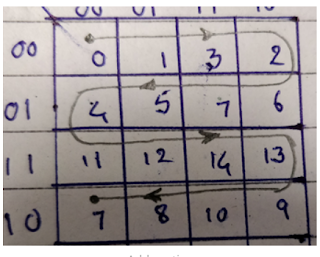
In grey counter only one bit is toggled at each time and this counter is used in pointing the memory locations and simple way to remember the grey count seqeunce


4-bit grey Counter
0000 – 0                                1101 – 12
0001 – 1                                1111 – 14
0011 – 3                                1110 – 13
0010 – 2                                1010 – 9
0110 – 6                                1011 – 10
0111 – 7                                1001 – 8
0101 – 5                                1000 – 7
0100 – 4
1100 – 11


Physical Cells :TAP CELLS, TIE CELLS, ENDCAP CELLS, DECAP CELLS

Tap Cells (Well Taps) :  These library cells connect the power and ground connections to the substrate and n­wells, respectively.  By plac...