Showing posts with label STA. Show all posts

Monday, 8 May 2023

CROSS TALK


Crosstalk noise: noise refers to undesired or unintentional effect between two or more signals that are going to affect the proper functionality of the chip. It is caused by capacitive coupling between neighboring signals on the die. In deep submicron technologies, noise plays an important role in terms of functionality or timing of device due to several reasons.
  • Increasing the number of metal layers. For example, 28nm has 7 or 8 metal layers and in 7nm it’s around 15 metal layers.
  • Vertically dominant metal aspect ratio it means that in lower technology wire are thin and tall but in higher technology the wire is wide and thin, thus a greater the proportion of the sidewall capacitance which maps into wire to wire capacitance between neighboring wires.
  • Higher routing density due to finer geometry means more metal layers are packed in close physical proximity.
  • A large number of interacting devices and interconnect.
  • Faster waveforms due to higher frequencies. Fast edge rates cause more current spikes as well as greater coupling impact on the neighboring cells.
  • Lower supply voltage, because the supply voltage is reduced it leaves a small margin for noise.
  • The switching activity on one net can affect on the coupled signal. The effected signal is called the victim and affecting signals termed as aggressors.

There are two types of noise effect caused by crosstalk
  • Glitch: when one net is switching and another net is constant then switching signal may cause spikes on the other net because of coupling capacitance (Cc) occur between two nets this is called crosstalk noise.
In fig the positive glitch is induced by crosstalk from rising edge waveform at the aggressor net. The magnitude of glitch depends on various factors.


  • Coupling capacitance between aggressor and victim net: greater the coupling capacitance, larger the magnitude of glitch.
  • Slew (transition) of the aggressor net: if the transition is more so magnitude of glitch also more. And we know the transition is more because of high output drive strength.
  • If Victim net grounded capacitance is small then the magnitude of glitch will be large.
  • If Victim net drive strength is small then the magnitude of glitch will be large.


Types of glitches:

  • Rise: when a victim net is low (constant 0) and the aggressor net is at a rising edge.

  • Fall: when a victim net is high (constant 1) and the aggressor net is at the falling edge.

  • Overshoot: when a victim net is high (constant 1)) and the aggressor net is at a rising edge.

  • Undershoot: when a victim net is low (constant 0) and the aggressor net is at the falling edge.


Crosstalk delay: 
when both nets are switching or in transition state then switching signal at the victim signal may have some delay or advancement in the transition due to coupling capacitance (Cc) occur between two nets this is called crosstalk delay.
Crosstalk delay depends on the switching direction of aggressor and victim net because of this either transition is slower or faster of the victim net.


Types of crosstalk:
Positive crosstalk: the aggressor net has a rising transition at the same time when the victim net has a falling transition. The aggressor net switching in the opposite direction increases the delay for the victim. The positive crosstalk impacts the driving cell, as well as the net, interconnect - the delay for both gets increased because the charge required for the coupling capacitance Cc is more.


Negative crosstalk: the aggressor net is a rising transition at the same time as the victim net. The aggressor's net switching in the same direction decrease delay of the victim. The positive crosstalk impacts the driving cell, as well as the net, interconnect - the delay for both gets decreased because the charge required for the coupling capacitance Cc is less.


Crosstalk effect on timing analysis:

Consider crosstalk in data path:
If the aggressor transition in the same direction as the victim then victim transition becomes fast because of this data will be arrive early means arrival time will be less.
Setup = RT – AT(dec) this is good for setup #dec- decrease
Hold = AT(dec) – RT this is bad for hold

If the aggressor transition in a different direction as a victim then victim transition becomes slow because of this data will be arrive late means arrival time will be more.


Setup = RT – AT(inc) this is not good for setup
Hold = AT(inc) – RT this is good for hold #inc- increase


Consider crosstalk in the clock path:
If the aggressor transition in the same direction as the victim then victim transition becomes fast because of this clock will be arrive early means Required time will be less.
Setup = RT(dec) – AT this is not good for setup
Hold = AT – RT(dec) this is good for hold

If the aggressor transition in a different direction as a victim then victim transition becomes slow because of this clock will be arrive late means the Required time will be more.
Setup = RT(inc) – AT this is good for setup
Hold = AT – RT(inc) this is not good for hold


How to reduce the crosstalk:
  • Wire spacing (NDR rules) by doing this we can reduce the coupling capacitance between two nets.
  • Increased the drive strength of victim net and decrease the drive strength of aggressor net
  • Jumping to higher layers (because higher layers have width is more)
  • Insert buffer to split long nets
  • Use multiple vias means less resistance then less RC delay
  • Shielding: high-frequency noise is coupled to VSS or VDD since shielded layers are connects to either VDD or VSS. The coupling capacitance remains constant with VDD or VSS.

Clock Uncertainty

Clock Uncertainty : The Time difference between the arrival of the clock signal at the register in one clock domain or between any two clock domains


Uncertainty is caused by following factors:
Clock Skew
  • Skew is the difference in clock arrival time across the chip.
  • Clock Skew is the temporal difference between the arrival of the same edge of a clock signal at the Clock pin of the capture and launch flops.
  • Signal takes time to move from one location to another. Clock latency is the time taken by a clock signal to move from the clock source to the clock pin of a particular flip-flop. Clock skew can alternatively be defined as the difference between capture and launch flop delay.
For example, The capture clock delay is 2.5ns while the launch clock latency is 0ns. The difference between them is 2.5ns-0ns = 2.5ns, which is the clock skew value

The clock should ideally reach the clock pin of all the flip-flops in a design at the same time, resulting in a zero skew. However, this is not attainable owing to varying wire-interconnect lengths and temperature changes.

What is the reason for skew in a design?
A skew in a design occurs when a flip-flop is put near the clock source and another flip-flop is placed at the far end of the core region. In practice, the skew cannot be zero due to the disparity in connecting lengths. To address this, a user-specified number is provided to obtain correct pre-CTS timing data. After the clock tree is constructed, the real skew values are accessible, and the uncertainty is limited to the Jitter value alone.

The time difference/delta between the launch flip flop and capture flip flop or
it refers to the absolute time diff between the clock signal arrival between the two points in the clock network

Tskew =Tlaunch_clk - Tcapture_clk

skew can be classified into different skews:
  •  +ve skew: Positive clock skew, In this case, the capture clock delay is greater than the launch clock latency. Positive skew is advantageous for setup timing. Due to the inclusion of skew, the capture clock is delayed by a few ns. Therefore the timing path requires one clock period and Skew margin to match the setup requirement.
  • -ve skew: Negative Skew is beneficial for hold time since it delays the fresh launch. Because of the delay in launching the new data, the prior data will be effectively recorded and will not be overwritten. However, negative skew is detrimental to setup timing.
  • Local skew: The disparity in latency between two related flops in a design is referred to as local skew.
  • Global skew: is the difference in clock delay between two unrelated flops or the difference between the longest and shortest clock paths in the design.
  • Usefull Skew :Useful skew is the skew that is purposefully introduced into the design to satisfy timing. It is particularly introduced in clock pathways where timing is failing, so that timing is passed in that path. However, useful skew cannot be applied arbitrarily. This must be done with caution, ensuring that the margin is accessible in both the preceding and subsequent time paths. The uncontrolled insertion of skew might result in further timing violations rather than resolving them. It may be used to correct both setups and hold errors 
Cock Jitter


It can be defined as “deviation of a clock edge from its ideal location.” Clock jitter is typically caused by clock generator circuitry, noise, power supply variations, interference from nearby circuitry etc. Jitter is a contributing factor to the design margin specified for timing closure.
Based on how it is measured in a system, jitter is of following types:
Period jitter
Period jitter is the deviation in cycle time of a clock signal with respect to the ideal period over a number of randomly selected cycles(say 10K cycles). It can be specified an average value of of clock period deviation over the selected cycles(RMS value) or can be the difference between maximum deviation & minimum deviation within the selected group(peak-to-peak period jitter).


Cycle to cycle jitter : 

C2C is the deviation in cycle of of two adjacent clock cycles over a random number of clock cycles. (say 10K). This is typically reported as a peak value within the random group.This is used to determine the high frequency jitter.


Phase jitter:

In frequency domain, the effect being measured is phase noise. It is the frequency domain representation of rapid, short-term, random fluctuations in the phase of a waveform. This can be translated to jitter values for use in digital design.


Please note all the above jitters are effectively the same phenomenon, but different way of measuring and representing the effect for use in design flow. The jitter number thus obtained is used to specify the design margin using the command “set_clock_uncertainty”.

Effects
Since the jitter affects the clock delay of the circuit and the time the clock is available at sync points, setup and hold of the path elements are affected by it. Depending on whether the jitter causes the clock to be slower or faster, there can be setup hold or setup violations in an otherwise timing clean system. This will in turn lead to performance or functional issues for the chip. So it is necessary that the designer knows the jitter values of the clock signal and need to be considered while analyzing timing.

Cross Talk
Swtiching of the signal in one net will effect the signal in neighboring net due to cross coupling capacitance, know as Cross Talk. This noise will affect the functionality of chip 

Wednesday, 15 January 2020

Recovery Time, Removal Time

Recovery Time:
Recovery time is the minmium time that as asynchronous control signal must be stable before the clock active- edge transition. In other words, this check ensures that after the asynchronous signal become inactive, there is adequate time to recover so that the next active clock edge can be effective.

Consider the time as show in below figure, between an asynchronous reset becoming inactive and the clock active edge of a flip-flop. If the active clock edge occurs too soon after the release of reset, in this case the state of the flip-flop may be unknow. Therefore it is required to have minimum time for asynshronus control signal to become stable. Recovery time is similar to setup time.


Removal Time:
Removal time is the minimum length of time that an asynchronous control must be stable after the clock active edge transition. This check ensures that the active clock edge has no effect because the asynchronus control signal remains active until removal time after the active clock edge.

Consider the asynchronous control signal is released(becomes inactive) well after the active clock edge so that the clock edge can have no effect. Similar to hold check, it is minimum path check except that it is on an asynchronous pin of flip flop.


Saturday, 28 September 2019

Setup time and Hold Time

Any digital design should be free from setup and hold violation. First, we will understand what is Setup and Hold time. Below fig is simple circuit with launch and capture flipflop, these are ideal flip flop (means setup time and hold time are zero)


Setup time is the minimum amount of time a synchronous data input should be held steady before the clock event so that the data input is reliably sampled by the clock event.
Hold time is the minimum amount of time a synchronous data input should be held steady after the clock event so that the data input is reliably sampled by the clock event.

Any design to work perfectly setup and hold slack must be positive. What is slack?
Slack is defined as difference between required arrival time to actual arrival time of the signal. There are setup and hold slack. Design works well if both the slacks are positive and there will be violation if any of them or both are -ve
Setup Slack is the difference between the Required time and Arrival time of the signal at capture flip flop. During the setup calculation we must take max delay values in data path and min values in clock path and the setup slack must be greater than zero for violation free circuit. Setup check is carried at next clock edge.

Setup slack=RT-AT
RT——-required time
AT——-arrival time
RT= clock_period(tp)+clock_network_delay(tc)-setup_time(tsu)
AT=flip_flop_delay(tc2q) +wire_delay(tw)+comb_delay(td)

Hold Slack is the difference between the Arrival time and the required time of the data signal. During the Hold calculation we must take min delay values in data path and max values in clock path and the hold slack must be greater than zero for violation free circuit. Hold check is done on same clock edge

Hold Slack =AT-RT
RT= clock_period(tp)+clock_network_delay(tc)+hold_time(th)
AT=flip_flop_delay(tc2q) +wire_delay(tw)+comb_delay(td)

Note: As hold analysis is carried on same clock, we must make clock_period to zero(tp=0)

How to we overcome the setup or hold violation
Setup violation occurs when the data arrives late at the capture flip flop and this can be avoided by reducing the delay in the data path. Delay in data path can be reduced in different steps

  • LVT cells offers less delay, we can swap the HVT cells to LVT cells
  • High drive strength cells delay is less compared to low drive strength and we can swap between the low drive strength cell to high drive strength cell, but we need compromise with the power.
  • If we can comprise with speed of the design, then clock frequency can be reduced to avoid the setup violation.

Hold violation occurs when the data arrives early at the capture flip flop and we need add delays in the data path to avoid the hold violation. We can do any of the steps to increase the delay in the data path    

  • We need to add the buffers in the data path
  • Swap HVT cells to LVT cells
  •  Swap high drive strength cells to low drive strength cells

Thursday, 26 September 2019

Drive Strength of devices

What is drive strength of device?
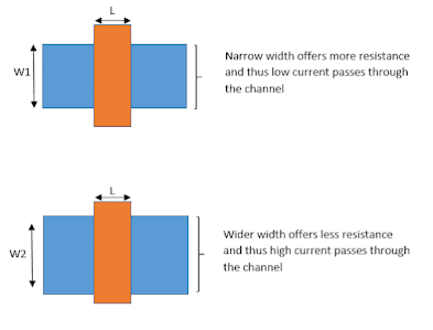
Drive strength is the current capability of the device, which is capable to drive the fan outs/output loads. The drive strength of the devices which is nothing but current carrying capacity can be increased by reducing the ON Resistance and Vice Versa. Thus ON resistance can be varied by varying two parameters of the devices

  • Width(W)
  • Channel Length(L)

Case: I 
ON Resistance is reduced with increasing the width of the channel as shown in the figure. W1 < W2, and L is same.

Width of the channel adds up to the height of the standard cell and if there is any restriction on the height of standard cell, we need to avoid changing width parameter of the cell/device(nmos or pmos).Instead we can the increase the width of the device indirectly by constructing more than one gates (fringes) and connecting them in parallel as show in below figure which increases effective width of the device.

The drive strength 1x, 2x, 3x … means width of the device is 1W, 2*W, 3*W respectively.

Case II
By changing the channel also we can change the driving strength!!!……. But for technology node channel length is constant, then how can channel length be changed?
For a given technology node there will be  more than one channel and this details are provided by fab people. I mentioned on channel length in my previous post Technology/Process Node
There raises a question when we need to upsize the drive strength?
When the load capacitance is more than the internal capacitance as a result charging time increases and delay increases, to reduce the charging time/delay we have to upsize the cell.

Clarification:
Lets us consider a CMOS design which has both nmos and pmos.The height of the cmos(standard cell) is equal to the sum of Vdd’s widht, pmos channel width, diffusion spacing between pull-up and pull-down transistors, nmos channel width and width of Vss metal layer. A clear picture was shown below. Thus changing the width of the channel in pmos or nmos effects the height of the standard cell

                                          CMOS LAYOUT

Where L represents the channel length of cell (pmos or nmos)
           W represents the channel width of cell(pmos or nmos)

False Paths:set_false_path

During the timing analysis, tools verifies whether logic paths meets all the constraints defined in the SDC (Synopsys design constraints) and reports violation if any logic paths doesn’t meet the required timings. And the tools are not intelligent enough to find which logic path was true or false path. Therefore, we must inform the tool which are the false paths before performing the timing analysis. Few cases are mentioned below.
Case I


During the Functional mode the select line of mux is tied to 0 and tool should not perform the timing analysis on this path (marked in orange) which will be active during DFT test mode. This information must be provided to the following command
set_flase_path -to <list of end points>


Case II:
We need to add false path on the pins which are tied to low or high (static signals). As they are static signals, timing checks are not necessary.
set_false_path -from [get_ports A]

Case III:
If two clocks are not related to each other (Asynchronous) then we must define these paths as false path. In this case to avoid any setup/hold violations at capturing registers some synchronizers technique must be employed. Few of the techniques are

  • Two flop Synchronizers
  •  FIFO
  •  Handshaking protocol

set_false_path -from CLKA   -to CLKB


In case of the two flip flop synchronizers as show in above figure timing checks are not necessary between the Launching flop and the 1st stage of the synchronizers. Therefore, we have to consider the signal to Flop FF2 as false path

Sunday, 22 September 2019

Clock Gating

Clocking gating is technique in which the clock signal is given to Flip Flop through AND/OR gate with enable signal as shown in fig 1. With this design there will be a glitch when the control signal is enabled after the clock rise edge. By using Integrated clock gating we can avoid the glitches.

                                                Fig 1: Simple clock gate

ICG is modification of a clock gating technique, and the enable/controls signal was synchronized with clock before gating the enable/control signal and clock signal to avoid the glitches and to reduce the dynamic power consumption. ICG with AND gate and negative flip flop is shown in fig 2. We can also use, OR gate and positive edge triggered flip flop to build a ICG. 

                                 Fig 2 : Integrated Clock Gating

Glitch free output is achieved from ICG circuit as shown in fig 3. And if we are not using the FF enable /control signal will not be synchronized with clock, which results a glitch in output. 


                                                  Fig 3 : Wave Form

Tuesday, 17 September 2019

Can hold violation be removed after chip was fabricated

Can we remove the hold violation once the chip was out from fabrication unit?
After the chip was manufactured, if there are any setup violations in the design, can removed by reducing the clock frequency of the design at the cost of device performance.Now if the hold violation was found after chip was out,we have to discard the the chip. Theoretically there are few methods to remove the hold violations, but in practical cases these may not be implemented on the chip

  1. By reducing the supply voltage and frequency, we can increase the delay of the cell and thus meet the hold violations
  2. By increasing the temperature, propagation delay of the cell decreases and thus we can met the hold violation. However for 65nm and below technology, temperature inversion phenomena was observed and thus delay decreases as temperature increased. For lower technology nodes increasing the temperature worsens the hold timing.

Physical Cells :TAP CELLS, TIE CELLS, ENDCAP CELLS, DECAP CELLS

Tap Cells (Well Taps) :  These library cells connect the power and ground connections to the substrate and n­wells, respectively.  By plac...