Monday, 30 September 2019

how to design the better transistor which has high on current and low off current

Speed of the transistor is decided with Ion and Ioff. On current was increased as we go down the technology node because less Vt is required for small channel length and delay of the device is also  reduced.When Device is off(i.e Vgs =0 and Vds=Vdd) there will be subthreshold current which contributes to the Ioff current and this current must be maintained low to reduce the static power. For better operation of the devices on current must be high and off current must be low.

  • Ion current was increased with decrease in Vt ( this is reduced for every latest technology node)
  • Ioff must be maintained low and this is achieved by reducing the subthreshold swing. Vt can be increased to reduce the Ioff but this will affect the Ion current of the device and delays of the devices will be affected.

Below image gives the equations of Ioff current and sub threshold swing 
W  represents the width of the channel
 L    represents the length of the channel
Vgs  represents the gate to source voltage
Cox  represents the oxide capacitance
 Vt represents the threshold voltage of the devices.


 From the above equations we can say Ioff can be reduced by changing S(subthershold swing) ,this can be achieved two ways

  • By Increasing the Cox i.e. using thinner oxide 
  • By reducing Cdep of the device, this can be done by increasing Wdep.
                                              nmos(source:internet)

Oxide capacitance can be increased by using the thinner oxide or high dielectric materials. Thickness of the oxide layers cannot be reduced beyond the 1nm , if it is beyond the 1nm , there will be a breakdown of the oxide material and tunnelling leakage current increases.
Because of the above limitation in thickness researchers started using the high K dielectric materials. Like 6nm thick HFO2 is equivalent to 1nm thick of Sio2 in the sense that both the films produce the same Cox. Like very solution as some negative effect, high K dielectrics are highly unstable and they react with the substrate.By inserting a thin Sio2 layer  between substrate and dielectric material the chemical reaction can be reduced. High K dielectric materials offer lower surface mobility than Si/Sio2 which is a disadvantage . 
Cdep can be reduced by increasing the Wdep, this can be done by decreasing the doping concentration because Wdep is inversely proportional to Nsub (doping concentration).
For a Device to work properly, we need to change Wdep, Tox, Xj(drain junction depth) proportional  to change in channel length 


Saturday, 28 September 2019

Setup time and Hold Time

Any digital design should be free from setup and hold violation. First, we will understand what is Setup and Hold time. Below fig is simple circuit with launch and capture flipflop, these are ideal flip flop (means setup time and hold time are zero)


Setup time is the minimum amount of time a synchronous data input should be held steady before the clock event so that the data input is reliably sampled by the clock event.
Hold time is the minimum amount of time a synchronous data input should be held steady after the clock event so that the data input is reliably sampled by the clock event.

Any design to work perfectly setup and hold slack must be positive. What is slack?
Slack is defined as difference between required arrival time to actual arrival time of the signal. There are setup and hold slack. Design works well if both the slacks are positive and there will be violation if any of them or both are -ve
Setup Slack is the difference between the Required time and Arrival time of the signal at capture flip flop. During the setup calculation we must take max delay values in data path and min values in clock path and the setup slack must be greater than zero for violation free circuit. Setup check is carried at next clock edge.

Setup slack=RT-AT
RT——-required time
AT——-arrival time
RT= clock_period(tp)+clock_network_delay(tc)-setup_time(tsu)
AT=flip_flop_delay(tc2q) +wire_delay(tw)+comb_delay(td)

Hold Slack is the difference between the Arrival time and the required time of the data signal. During the Hold calculation we must take min delay values in data path and max values in clock path and the hold slack must be greater than zero for violation free circuit. Hold check is done on same clock edge

Hold Slack =AT-RT
RT= clock_period(tp)+clock_network_delay(tc)+hold_time(th)
AT=flip_flop_delay(tc2q) +wire_delay(tw)+comb_delay(td)

Note: As hold analysis is carried on same clock, we must make clock_period to zero(tp=0)

How to we overcome the setup or hold violation
Setup violation occurs when the data arrives late at the capture flip flop and this can be avoided by reducing the delay in the data path. Delay in data path can be reduced in different steps

  • LVT cells offers less delay, we can swap the HVT cells to LVT cells
  • High drive strength cells delay is less compared to low drive strength and we can swap between the low drive strength cell to high drive strength cell, but we need compromise with the power.
  • If we can comprise with speed of the design, then clock frequency can be reduced to avoid the setup violation.

Hold violation occurs when the data arrives early at the capture flip flop and we need add delays in the data path to avoid the hold violation. We can do any of the steps to increase the delay in the data path    

  • We need to add the buffers in the data path
  • Swap HVT cells to LVT cells
  •  Swap high drive strength cells to low drive strength cells

Friday, 27 September 2019

Design For Testability

DFT means Design for testability, where logic will be implemented or inserted in the core design at RTL stage(Now a days most of the company prefer at RTL stage) or Netlist stage. This test circuit verifies that core design does not have manufacturing defects focusing on circuit structure rather than functional behavior.

Manufacturing defects may include

  • Short circuits
  • Open interconnects
  • Power and ground shorts

Manufacturing defects remain undetected by functional testing and these can cause undesirable behaviour during circuit operation. DFT helps to find the manufactured defects and improves the quality, yield of products.

Now you may wonder what is the use of Functional testing.Functional testing verifies your circuit performs .For example assume that your design is an Half adder circuit , Functional test verifies that circuit performs the addition operation and computes the correct results over the range of patterns

Thursday, 26 September 2019

Temperature effects on Mobility

In a Cmos or Finfet the current flow is due to movement of the electrons and holes. The free movement depends on the mobility of electrons/holes and factors affects the mobility are lattice scattering and impurity scattering which are dependent on the temperature.

Lattice scattering
Atoms vibrate more as the temperature increase and this results in collisions with another atoms and causing carriers (electrons/holes) to be free. This collective vibration is called phonon, thus it is also called as phonon scattering. Therefore with increase in temperature the vibrations of atoms increases and more carries are scattered from atoms, this increases the collision between the electrons and reduces the mobility. Despite the decrease in mobility, conductivity increase with the temperature as carrier concentration increases with temperature. Mathematical relation between the mobility and temperature as follows


 Impurity scattering
Impurity scattering is observed in the doped semiconductors. At room temperature the impurities are ionized, and there is electrostatic attraction between the electrons travelling in the lattice and the impurities. As temperature increases the mobility of electron increased which is quite opposite to the Lattice scattering. Impurity scattering is more dominate only at low temperature in doped semiconductors. For better understanding, the electron can travel faster with increase in the temperature and it can escape the attraction forces of the impurity ions. Mathematical relation between the mobility and temperature as follows


we can observe only lattice scattering in intrinsic semiconductor where as in doped conductors we can see lattice and impurity scattering which effects the mobility of the electrons/holes.

In less doped semiconductors, the lattice scattering dominates and thus mobility decrease with increase in temperature.

For heavily doped semiconductors at low temperature as temperature increases the mobility of electrons increases since impurity scattering dominates and at high temperature the mobility decrease since lattice scattering dominates

                                           source: Image from google

Drive Strength of devices

What is drive strength of device?
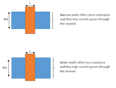
Drive strength is the current capability of the device, which is capable to drive the fan outs/output loads. The drive strength of the devices which is nothing but current carrying capacity can be increased by reducing the ON Resistance and Vice Versa. Thus ON resistance can be varied by varying two parameters of the devices

  • Width(W)
  • Channel Length(L)

Case: I 
ON Resistance is reduced with increasing the width of the channel as shown in the figure. W1 < W2, and L is same.

Width of the channel adds up to the height of the standard cell and if there is any restriction on the height of standard cell, we need to avoid changing width parameter of the cell/device(nmos or pmos).Instead we can the increase the width of the device indirectly by constructing more than one gates (fringes) and connecting them in parallel as show in below figure which increases effective width of the device.

The drive strength 1x, 2x, 3x … means width of the device is 1W, 2*W, 3*W respectively.

Case II
By changing the channel also we can change the driving strength!!!……. But for technology node channel length is constant, then how can channel length be changed?
For a given technology node there will be  more than one channel and this details are provided by fab people. I mentioned on channel length in my previous post Technology/Process Node
There raises a question when we need to upsize the drive strength?
When the load capacitance is more than the internal capacitance as a result charging time increases and delay increases, to reduce the charging time/delay we have to upsize the cell.

Clarification:
Lets us consider a CMOS design which has both nmos and pmos.The height of the cmos(standard cell) is equal to the sum of Vdd’s widht, pmos channel width, diffusion spacing between pull-up and pull-down transistors, nmos channel width and width of Vss metal layer. A clear picture was shown below. Thus changing the width of the channel in pmos or nmos effects the height of the standard cell

                                          CMOS LAYOUT

Where L represents the channel length of cell (pmos or nmos)
           W represents the channel width of cell(pmos or nmos)

False Paths:set_false_path

During the timing analysis, tools verifies whether logic paths meets all the constraints defined in the SDC (Synopsys design constraints) and reports violation if any logic paths doesn’t meet the required timings. And the tools are not intelligent enough to find which logic path was true or false path. Therefore, we must inform the tool which are the false paths before performing the timing analysis. Few cases are mentioned below.
Case I


During the Functional mode the select line of mux is tied to 0 and tool should not perform the timing analysis on this path (marked in orange) which will be active during DFT test mode. This information must be provided to the following command
set_flase_path -to <list of end points>


Case II:
We need to add false path on the pins which are tied to low or high (static signals). As they are static signals, timing checks are not necessary.
set_false_path -from [get_ports A]

Case III:
If two clocks are not related to each other (Asynchronous) then we must define these paths as false path. In this case to avoid any setup/hold violations at capturing registers some synchronizers technique must be employed. Few of the techniques are

  • Two flop Synchronizers
  •  FIFO
  •  Handshaking protocol

set_false_path -from CLKA   -to CLKB


In case of the two flip flop synchronizers as show in above figure timing checks are not necessary between the Launching flop and the 1st stage of the synchronizers. Therefore, we have to consider the signal to Flop FF2 as false path

Sunday, 22 September 2019

Clock Gating

Clocking gating is technique in which the clock signal is given to Flip Flop through AND/OR gate with enable signal as shown in fig 1. With this design there will be a glitch when the control signal is enabled after the clock rise edge. By using Integrated clock gating we can avoid the glitches.

                                                Fig 1: Simple clock gate

ICG is modification of a clock gating technique, and the enable/controls signal was synchronized with clock before gating the enable/control signal and clock signal to avoid the glitches and to reduce the dynamic power consumption. ICG with AND gate and negative flip flop is shown in fig 2. We can also use, OR gate and positive edge triggered flip flop to build a ICG. 

                                 Fig 2 : Integrated Clock Gating

Glitch free output is achieved from ICG circuit as shown in fig 3. And if we are not using the FF enable /control signal will not be synchronized with clock, which results a glitch in output. 


                                                  Fig 3 : Wave Form

Physical Cells :TAP CELLS, TIE CELLS, ENDCAP CELLS, DECAP CELLS

Tap Cells (Well Taps) :  These library cells connect the power and ground connections to the substrate and n­wells, respectively.  By plac...